Products
Giới thiệu sản phẩm
Elec-Beam Machinery
X-eye 6100
작성자 관리자
날짜 2023-07-24 14:42:09
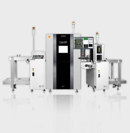
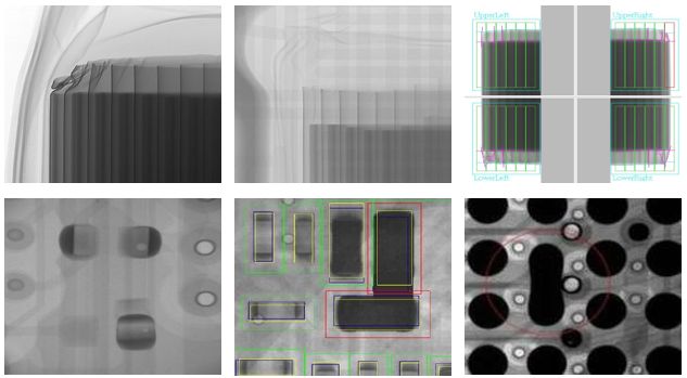
Automatically In-Line inspect Solder Joint defects of PCBA, and other defects on Hidden Components.
Able to be customized regarding Application by users setting ROIs.
Especially, area-type image scanning can gain high resolution results fast.
- High speed 2D In-Line Inspection System (0.5 sec/FOV)
- Various defect inspection - BGA, Chip, QFN, QFP, etc.
| General Product Features | |
|---|---|
| X-ray Tub | 100㎸ / 200㎂ |
| Min Resolution | 5㎛ |
| Table Size | 400 x 400mm |
| Detector | 5 inch FPXD |
| 검사 대상 | BGA, Chip, QFN, QFP |
| 검사 항목 | BGA : Short, Bridging, Void Chip : Manhattan, Miss align, Short |
| Dimension | 1,020(W) x 1,350(D) x 1,720(H)mm / 1,500kg |
X-Ray Image
댓글 (0)
등록된 댓글이 없습니다.